Laser Marking
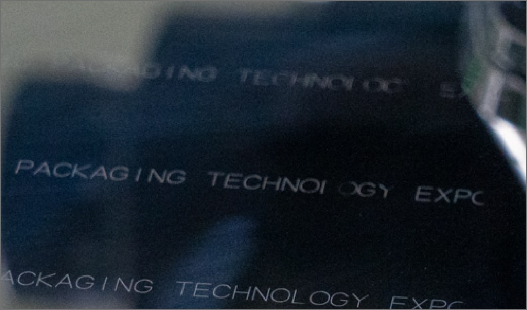
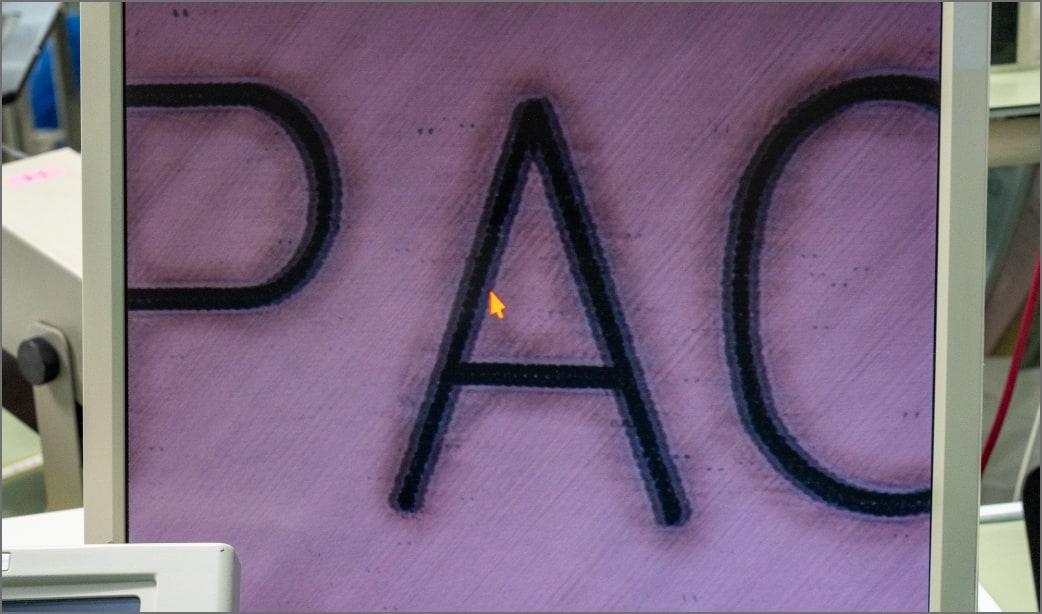
Traceability for Each Die is Available
by Laser Marking on the Backside of Wafers.
Examples
Model, Lot No, Company Name, Logo Mark, Wafer Slot Number, Address, etc.
Marking Materials
Silicon wafer


Equipment
| Equipment | Wafer Size | Number | Specification | Note |
|---|---|---|---|---|
| Laser Marking | 6/8 inch | 2 | Supported Wafer Thickness: 200μm (200μm or less, please consult us) Character Size: about 0.3mm ~ |
Shibaura Mechatronics (LAY-701ASAB) |
Marking without Flexural Strength Decrease
By optimizing Laser output, Frequency, and the Location of Marking, we can prevent Flexural Strength decrease caused by Laser Marking.
About Laser Marking Requests
Main Information Required When Making Requests
- Chip Size
- Wafer Size
- Contents, Size, and Position of Characters
- Wafer Materials
Introduction Flow of Laser Marking
STEP01
Judgment of Whether Processing Is Possible
Along with the processing information above, please provide us with a drawing (handwritten or digital) of what kind of marking you want to do, and we will judge whether processing is possible.
STEP02
Processing Test
The customer provides a wafer sample and performs laser marking test processing based on the specifications.
STEP03
Confirmation of Processing Test
Please check the results of the processing test.
STEP04
Mass Production
If the test product passes the test, we shift to a mass production system and carry out laser marking for the requested quantity.
STEP05
Delivery of Materials
We will deliver the product to the customer after completing the mass production process.
*From Step 1 to Step 5, it will take about 1 week at the shortest. Please inquire about the delivery date.